Canon Lithography Systems
Canon Photolithography systems are designed to provide exceptional performance, quality and cost of ownership for wafer and panel processes requiring high-precision patterning for the fabrication of cutting-edge technology.
LITHOGRAPHY SYSTEMS AND SOLUTIONS
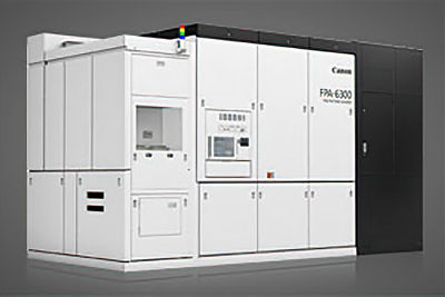
Front-end i-Line Steppers
Canon has a comprehensive lineup of i-line lithography equipment for semiconductor manufacturers to support the growth of 5G, RF, Power and Internet of Things (IoT) devices. Canon i-line steppers can handle wafer sizes from 50 mm to 300 mm. 3030 Body steppers can be configured with a multi-wafer handling kit that allows manufacturers to switch between two wafer sizes for fabrication of multiple devices within one stepper.
Advanced Packaging Steppers
New Advanced Packaging challenges are emerging including demands for higher resolution, larger exposure field size, improved overlay compensation and adoption of panel-substrates to reduce total process costs. Canon combines our 50 years in the semiconductor equipment industry with our ability to design precision optics for front-end chip fabrication industry to create solutions for Advanced Packaging.
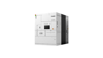
KrF Scanners and Steppers
Supporting the growth of the logic, memory and CMOS Image Sensor and and IoT markets, Canon KrF lithography systems utilize a DUV (248 nm) exposure light source with options available to allow handling of wafers from 50 mm to 300 mm in diameter. Canon KrF systems can enable low cost-of-ownership for leading edge processes while providing increased performance and productivity to extend legacy production lines.
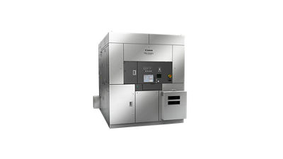
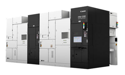
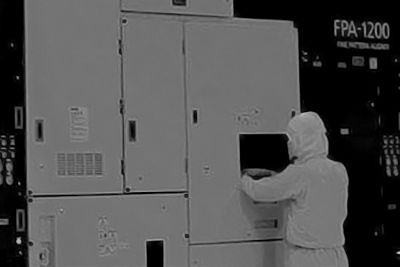
Nanoimprint Lithography
FPA-1200NZ2C systems utilize high-resolution imprint masks that can faithfully reproduce fine circuit patterns on the wafer. Nanoimprint Lithography (NIL) equipment forms patterns on wafers by pressing a mask containing circuit patterns into resist in an imprint process. FPA-1200NZ2C nanoimprint lithography systems support ≤ 15 nanometer processes and can offer benefits over traditional photolithography equipment that can be susceptible to optical distortion.
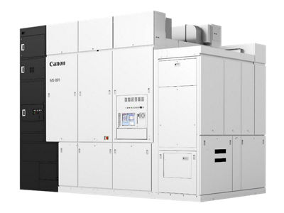
Wafer Measurement
Canon’s MS-001 wafer metrology system is capable of measuring the position of hundreds of alignment marks on semiconductor wafers in advance of wafer patterning. Premeasuring the alignment mark positions can result in improved overlay accuracy and reduced alignment measurement time in the lithography process.
The MS-001 allows the majority of alignment measurements to be performed in one batch process, outside of the lithography system. The productivity of the lithography system can be improved by reducing the number of measurements performed.
CANON REFURBISHED EQUIPMENT
Canon CPO Equipment Program: Refurbished Photolithography Equipment Solutions
Canon CPO Equipment Programs offers lower cost alternatives to purchasing new equipment. Through these programs, Canon U.S.A. aims to reduce the costs and risks that may occur with third party installation of used Canon photolithography equipment. Canon U.S.A. works together with its global affiliates to deliver outstanding equipment performance, quality and price with the reliability of Canon support and approved dealers.

DO YOU HAVE QUESTIONS ABOUT OUR LITHOGRAPHY PRODUCTS?
Semiconductor Manufacturing Equipment and Industrial Products Catalog
Browse our catalog to view the entire list of products.

TECHNOLOGY BEHIND LITHOGRAPHY EQUIPMENT
Canon Nanoimprint Lithography